
Here is a summary of some key PCB design guidelines and best practices for robust, reliable and cost-effective IoT hardware:
- Optimize component placement for compactness, considering proximity of connected sections.
- Provide adequate thermal reliefs and heat sinks if high power dissipation is expected.
- Include test points, programming and debug provisions for easy troubleshooting.
- Maintain controlled impedance for traces carrying high speed data.
- Use wider traces and polygons on inner layers for power distribution.
- Design with manufacturing and assembly in mind. Allow sufficient tolerances and spacing.
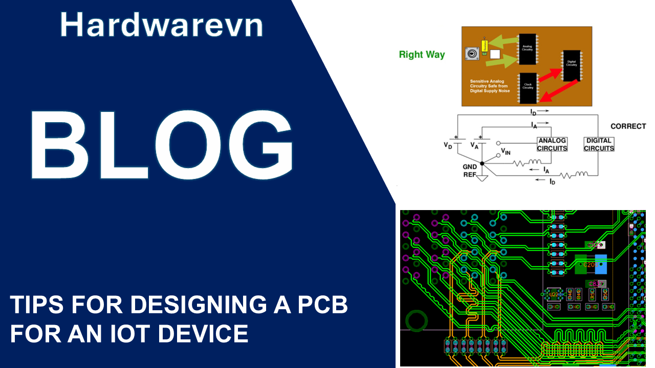
- Reduce analog circuit noise through isolation, shielding and filtering.
- Verify critical parameters through simulation during the design stage.
- Validate PCB performance under expected environmental conditions.
- Work closely with fabrication and assembly partners to avoid manufacturability issues.
How can EMI/EMC issues be minimized in an IoT PCB design?
Some ways to minimize EMI/EMC issues in IoT PCB design:
- Use shielding enclosures for sensitive analog and RF circuits.
- Include metal/graphite gaskets between mating surfaces of enclosure.
- Use common ground planes. Minimize ground loops. Provide multiple layer-to-layer ground vias.
- Isolate noisy digital circuits from sensitive analog sections.
- Use bypass/decoupling capacitors near every IC to filter noise.
- Add ferrite beads and other passive filter components on I/O lines.
- Keep high speed trace lengths short. Use controlled impedance routing.
- Avoid slots/cutouts on ground planes below critical traces.