
Checklist for PDN
Although this list is not inclusive of every parameter and variable that must be considered when designing a PCB, a PDN-optimized PCB design will implement these guidelines:
❏ Power and ground plane pairs (or “islands”) should be closely coupled together. The capacitance formed between the planes can be used to decouple the power supply at high frequencies.
❏ Whenever possible, the power and ground planes should be solid as this provides a continuous return path for return current.
❏ Use a thin dielectric thickness between the power and ground plane pair. Capacitance is inversely proportional to the separation of the plane pair so minimizing the separation distance (such as, the
dielectric thickness) will maximize the resulting capacitance.
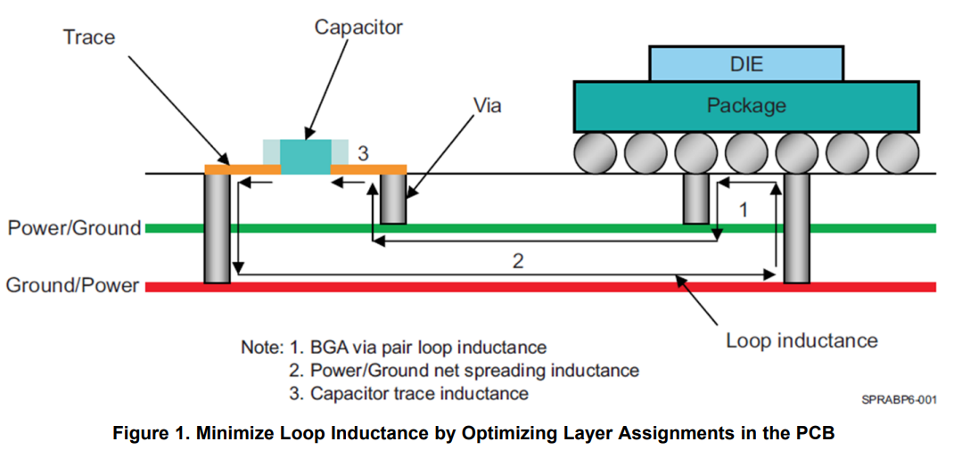
❏ The placement of power and ground planes in the PCB stack-up (determined by layer assignment) has a significant impact on the parasitic inductances of power current path. For this reason, it is
recommended to consider layer order in the early stages of the PCB PDN design cycle, placing high priority supplies in the upper-half of the stack-up and low priority supplies in the lower half of the stackup. This helps to minimize the loop inductance caused by decoupling capacitors and their associated vias.
❏ External power trace routing between components should be as wide as possible as wider traces result in reduced DC resistance and consequently a lower static IR drop.
❏ Whenever possible, attempt to achieve a ratio of 1:1 (or better) for component pins and associated vias. Do not share vias among multiple capacitors.
❏ Placement of decoupling capacitors and their associated vias should be as close to the processor ball as possible. Reserve the space directly underneath the processor for this purpose.
❏ Use of short and wide surface traces to connect capacitor pads to the vias connected to the planes below is preferred.
❏ Use of large diameter vias is preferred for reduced inductance/resistance.
❏ 1 oz – 2 oz Cu weight for power / ground plane is preferred to enable better PCB heat spreading, which helps to reduce processor junction temperatures. In addition, it is preferable to have the power /
ground planes be located adjacent to the PCB surface on which the processor is mounted.
❏ Place the VRM as close as possible to the processor and on the same side of the PCB. In cases where a power management IC (PMIC) is implemented as the VRM, it should be aligned to minimize distance for the highest current rail.
Tham khảo: 66AK2G1x: EVMK2GX General Purpose EVM Power Distribution Network Analysis