Ảnh hưởng của thành phần điện dung trong linh kiện TVS có ảnh hưởng đến chất lượng tín hiệu highspeed, điện dung này được khuyên nghị càng nhỏ càng tốt.


Layout Considerations:
Board layout is an important factor to get the best system performance in protection and other aspects like signal integrity. By following these ESD layout guidelines it can be ensured that the protection device gets
optimum performance in the system.
• General ESD layout best practices:
– In order to discharge the ESD before it couples onto anything close to it, place the protection devices as near to the connector as design rules allow
– Place the Protected IC much further from the protection device than the protection device is to the connector
– Do not use stubs between the ESD source and protection device, route directly from the ESD source to protection
– In order to conduct most current into the ESD device and keep the clamping voltage low, minimize any inductance between the ESD Source and the path to ground through the TVS
• Use a grounding scheme that has very low impedance:
– Connect the protection device Ground Pin directly to a same layer ground plane that has nearby VIAs stitching to an adjacent internal ground plane
– Use multiple ground planes when possible
– Use VIAs of large diameter with a large drill, which lowers impedance
• Limit the effects of EMI on unprotected circuits:
– Do not route unprotected circuits in the area between the ESD Source and the TVS to minimize EMI coupling onto unprotected traces
– Route with straight traces between the ESD Source and the protection device if possible
– Avoid using sharp corners in routing since electric fields tend to build up on corners, increasing EMI coupling
Also, the number of VIAs should be kept to minimum for high speed data lines. Take USB Type-C data lines as an example (Figure 6), there are four SuperSpeed TX-RX data lines on each end of the connector. This is split into four on each side of a two-layer board. A four-channel ESD device is a popular choice for many applications, but for Type-C connectors that have 20-Gbps differential pairs it may not be the best option since VIAs are needed to route all four data lines to the same layer. This issue can be mitigated by using single or dual channel ESD devices.

Example Layout with 4-Channel Routing Inefficiencies

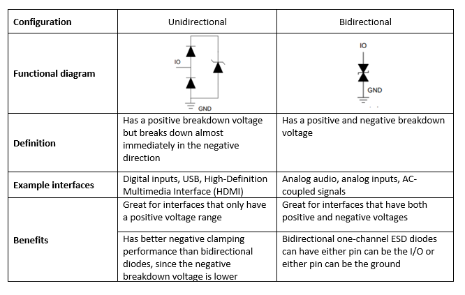
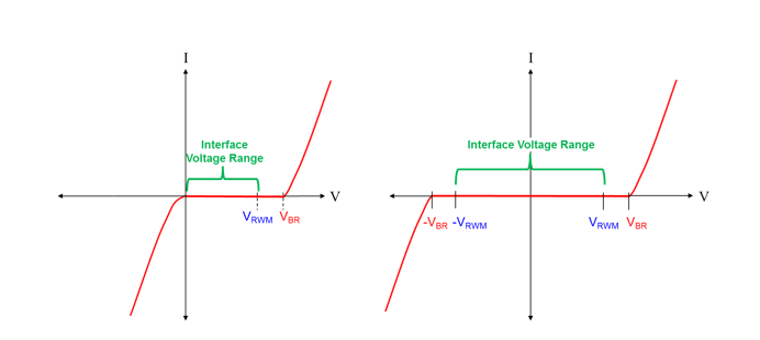
So sánh giữa TVS một chiều và TVS 2 chiều


Tham khảo bài viết:
https://e2e.ti.com/blogs_/b/analogwire/posts/esd-fundamentals-part-4-esd-capacitance
https://www.ti.com/lit/sg/sszb130d/sszb130d.pdf

